March 4, 2024
New spiral Contact Lenses can Correct Vision and Have Other Technological Uses
New spiral Contact Lenses can Correct Vision and Have Other Technological Uses
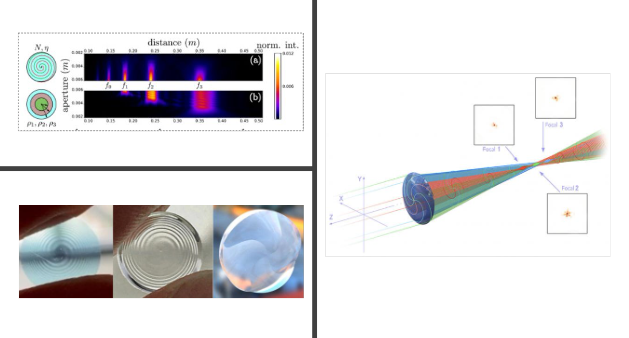
A new spiral shaped contact lens design can correct vision and the technology could also be applied to a range of miniaturized imaging systems such as those used for drones or self-driving cars. Consumer gadgets such as VR headsets could also benefit from the technology. The lens is called a spiral diopter, and it was created through a collaboration of French researchers from various companies and institutions including Optica, SPIRAL SAS, and the Photonics, Numerical and NanoSciences Laboratory (LP2N). The lens works by channeling incoming light and making it spin in an optical vortex, which improves the negative effects of various deformations in the cornea of the eye that can form as we age. Currently people use progressive lenses to focus their vision at different distances and combat conditions such as farsightedness and cataracts. In progressive lenses different parts of the lens have different magnifications and the user can experience distortions around their peripheral vision. The spiral diopter with its much more compact design enables visual focus at different distances, and thanks to the use of a spiral design based of Fermat’s spiral, it avoids distortions around the wearer’s peripheral vision. Learn more about this topic here.
March 19, 2024
Breakthrough in the Semiconductor Industry: First Ever N-type Diamond MOSFET is Created
Breakthrough in the Semiconductor Industry: First Ever N-type Diamond MOSFET is Created
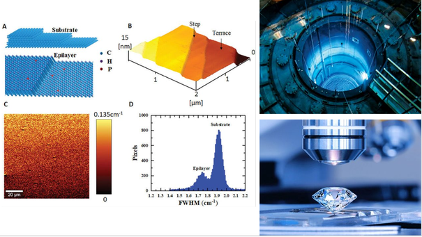
A team of researchers produced the world’s first n-channel diamond metal-oxide-semiconductor field-effect transistor (MOSFET). A key step toward diamond power electronics and integrated circuits for harsh environments. Semiconductor diamond has excellent physical characteristics including ultra-wide-bandgap energy of 5.5 eV, high carrier mobilities, and high thermal conductivity. Such properties have great potential for applications in extreme environmental conditions that require high reliability and high performance. For example, semiconductor diamond could be used in proximity to nuclear reactor cores that emit intense heat and high levels of radiation. Furthermore, the use of diamond electronics will reduce the need for thermal management and such devices would also be more energy efficient and could handle higher breakdown voltages and harsher environments. The fabrication of CMOS (complementary metal-oxide-semiconductor) Integrated circuits requires both p and n- type channel MOSFETs for conventional silicon electronics. The issue was that n-channel MOSFETs hadn't been created yet. However, a research team at the National Institute for Materials Science (NIMS) recently made a significant achievement by developing a method to grow high-quality diamond semiconductors with smooth flat terraces at the atomic level, which the achieved by doping the diamond with a low concentration of phosphorus. Learn more about this topic here.


